 The Society of Robotics and Automation is a society for VJTI students. As the name suggests, we deal with Robotics, Machine Vision and Automation
TinyGPU - custom RVV GPU
Author: Atharva Alulkar
TinyGPU
1. Introduction
This is a custom RVV compliant 64 bit parallel processor written in Verilog/ SystemVerilog. RISC-V Vector Extension 1.0 is a spec sheet made for having a simpler ISA for SIMD or Vector Processor designs.
I integrated it with the CVA6 CPU which offloads all vector extension from the CPU to the coprocessor. We compared benchmarks like matrix multiplication and matrix addition for the CPU and GPU and got a real speedup.
TinyGPU follows a SIMD style architecture with three memory buffers similar to what I saw in Nvidia’s CUDA architecture for their GPUs. There are 4 SIMD cores each with 4 ALU lanes and a decoder that sits on top of it all.
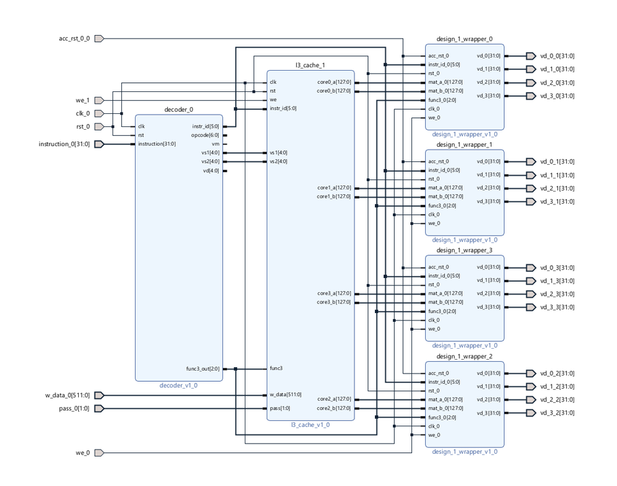
2. TinyGPU insides
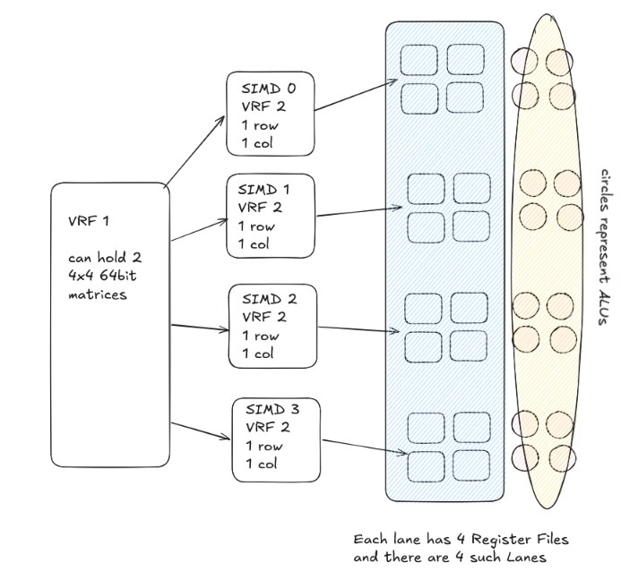
As I said TinyGPU has 3 levels of memory hierarchy which is the most distinct pattern about this design. They go as follows:
- L1 cache (VRF1) - holds both the input matrices (1024 bit x 2).
- L2 cache (VRF2) - private to one SIMD core only - stores 1 row and 1 column from matrix A and Brespectively
- Register Files (VRF3) - private to each ALU lane, holds two 64 bit elements that the ALU computes. These usually repsresent the output matrix C elements.
This type is often seen in NVIDIA CUDA architectures where you have a shared cache, stream multiprocessors (SM) have their own vector registers as well.
3. The ALU and Decoder
TinyGPU has its own ALU that can do only Integer type operations for now (because of the FPGA limiation, which I will discuss later). The ALU can do:
- Add
- Sub
- Mul (signed, unsigned, higher upper)
- Div (signed)
- Matrix Multiplication (vmacc.vv)
Implementing the Mul and Div was a task due to Vivado bloating up the ALU to 900 LUTs!!
The decoder is set to decode standard RVV opcode, with the func3 and func7 mixing created as well. It separates the instrucions into two broad categories - VMACC.vv and NON-VMACC.vv. This is done so that the design properly aligns the data into rows (for non vmacc op) or rows and columns (for vmacc.vv op). This is done by padding in the VRF 1 itself.
4. CVA6
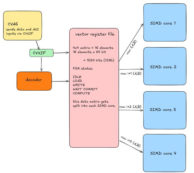
CVA6 is a RISC-V CPU designed by OpenHW in ETH Zurich. It is used in a lot of research projects for its indepth architecture and support from community. ARA is a vector coprocessor made for CVA6 using the CV-X-IF protocol. It stands for CoreV-eXtension-Interface and it is a modification on the AXI protocol that also has its own set of rules on how to use it, how does data transmit from CVA6 to the accelerator you have made.
In basic:
CVA6 sees RVV instruction -> CVA6 pipeline reaches execute -> RVV is marked as illegal (1) and CVXIF is set to ENABLE (also 1) -> CVA6 sees 1&1 from both -> offloads instruction and data to TinyGPU
5. FPGA Utilisation and Vivado reports
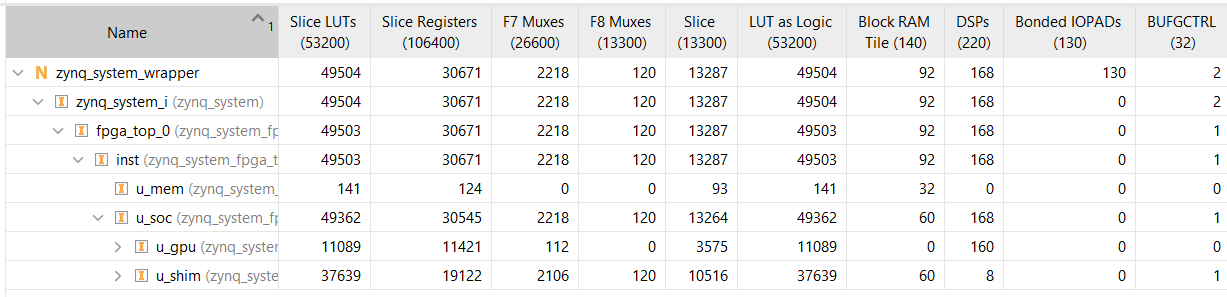
This project was run on the Zynq zc702 FPGA which has support for UART. The output was produced using Vitis IDE on a serial monitor where we use mcycle count for checking the speedup. This section deals only with the FPGA utilisation but I felt it necessary to include detail on how the “output” is captured as well.
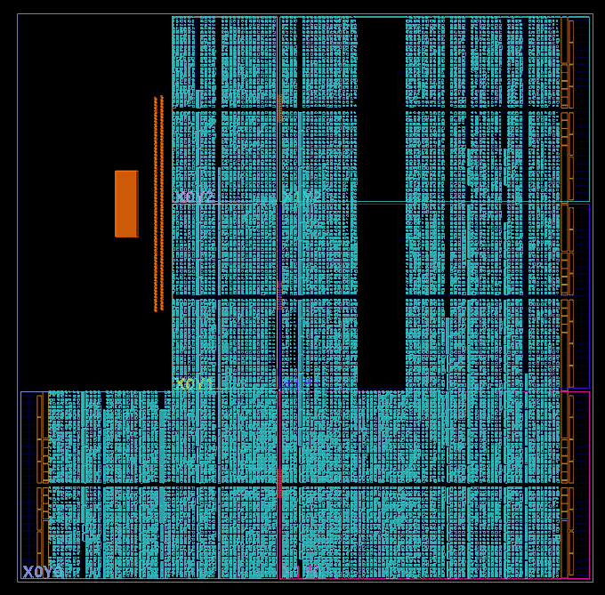
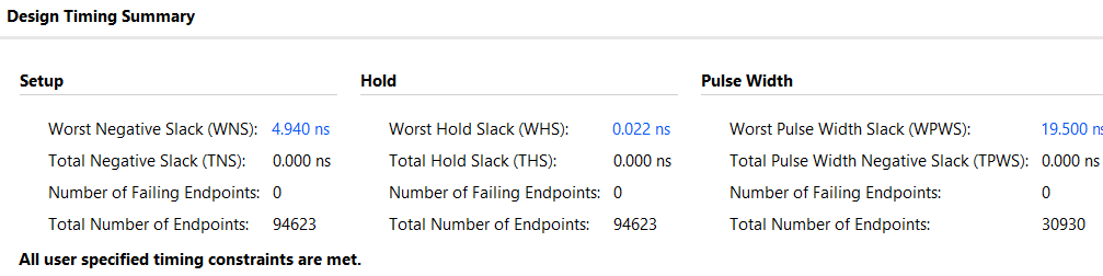
While doing this project I was also exposed to reading Vivado reports like the timing closure, power utilisation, node overlap, etc. These are all important things that I feel some one working on chip design should be able to understand and make sense of - and it has to be a personal quest. I will not elaborate on what each term means since it will be a big miss in someone else’s learning.
FPGA Utilisation
Timing Summary
Power Usage Report
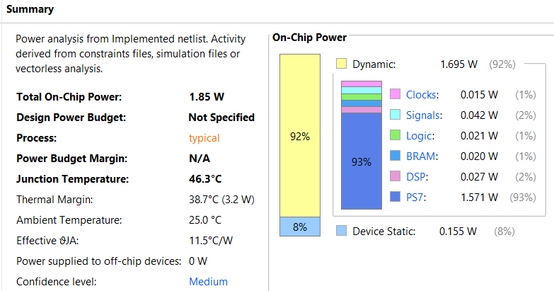
As we see, all the reports report successful Vivado implementation and now I can focus on the output and cycle count side of the project.
6. Output, Mcycle count, Vitis
We have shown output for 2 operations - matrix multiplication and addition. The benchmark is done by comparing mcycle ie the delta between when the operation starts and ends.
To understand this, if TinyGPU starts matmul at 100ns and ends at 150ns the mcycle count is 50 / clock_cycle = 50/10 = 5 therefore it needs 5 clock cycles at 10ns to compute the output of a 4x4 matrix multiplication. And the same for CVA6
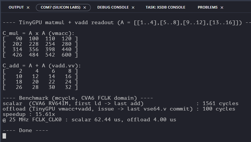
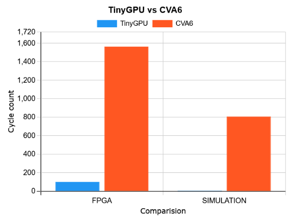
Thus, we got the output from the FPGA and displayed it on a serial monitor in the Vitis IDE using UART cable. The speed up offered is as follows:
- FPGA speed up: 15.61x compared to CVA6 at 25MHz F_CLCK
- Simulation speed up: 161.2x compared to CVA6 at 100MHz
7. Conclusion
From this project I learnt about the details of computer architecture and about chip design, I have demonstrated practical use of a GPU for use cases like matrix operations which have application in ML or in graphic processing. I also show how a vector accelerator can be used in tandem with a CPU to get faster results on highly parallelisable operations and shown the speed up offered on real hardware (FPGA).