 The Society of Robotics and Automation is a society for VJTI students. As the name suggests, we deal with Robotics, Machine Vision and Automation
Further updates on RISC-V CPU
What have we done so far?
With 3 weeks of brainstorming through countless internet resources, books, and websites we can finally say that we have acquired the knowledge we would need to complete the CPU. By the time of 1st week, we completed an edx course related to RISC-V-based CPU implementation through TL-Verilog.
Although we use Verilog as our base language the main aim of this course was to acquire knowledge of RISC-V architecture and learn the basics of hardware implementations as we set a strong foot in the world of registers, wires, and binary numbers. As we completed the course and got ourselves a brief idea of what was to come ahead we started learning Verilog language (this one we are going to use). Through this time we not only learned the Verilog Syntax but also started to understand how the hardware acts based on given instructions and its general behaviour throughout. In the upcoming weeks, we mastered Verilog basics and implementations, thanks to our previous knowledge of TL-Verilog and other programming languages.
Over the last weeks, we researched the working of each working module in a CPU and tried to imitate it through Verilog codes (I like to think we did a good job there). But the task wasn’t over as we were not only supposed to write the code but also were to write a testbench code to check whether the said module performs the said task perfectly.
As the module codes were implemented we also challenged ourselves by adding the M(multiplication) extensions for the instructions making a total of 47 executable instructions for the CPU to perform. Last but not least we connected all the modules (Verilog codes) through intel powered application namely Quartus to generate a detailed blueprint of a fully functioning CPU.
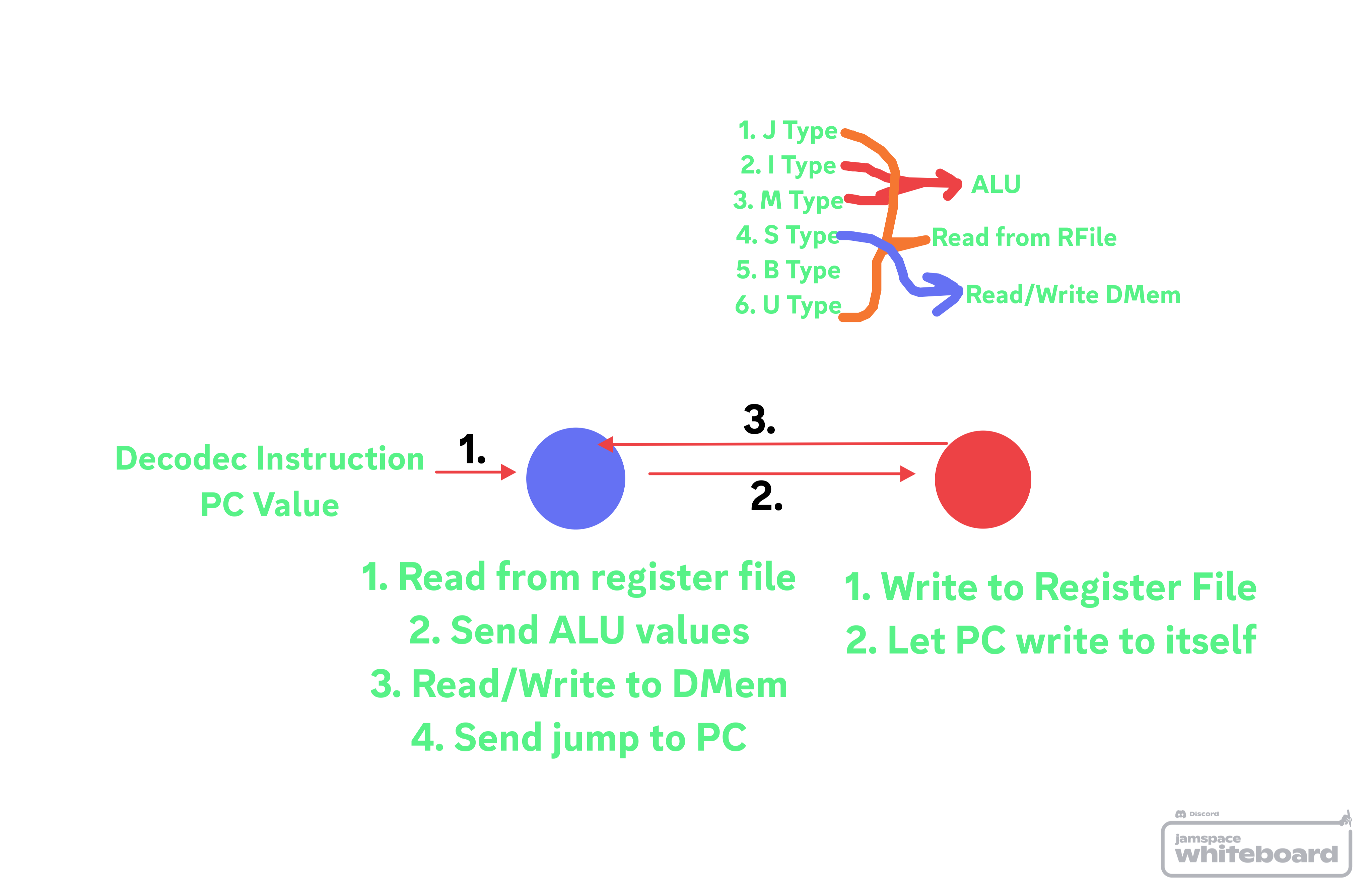
Control flow diagram of Control unit
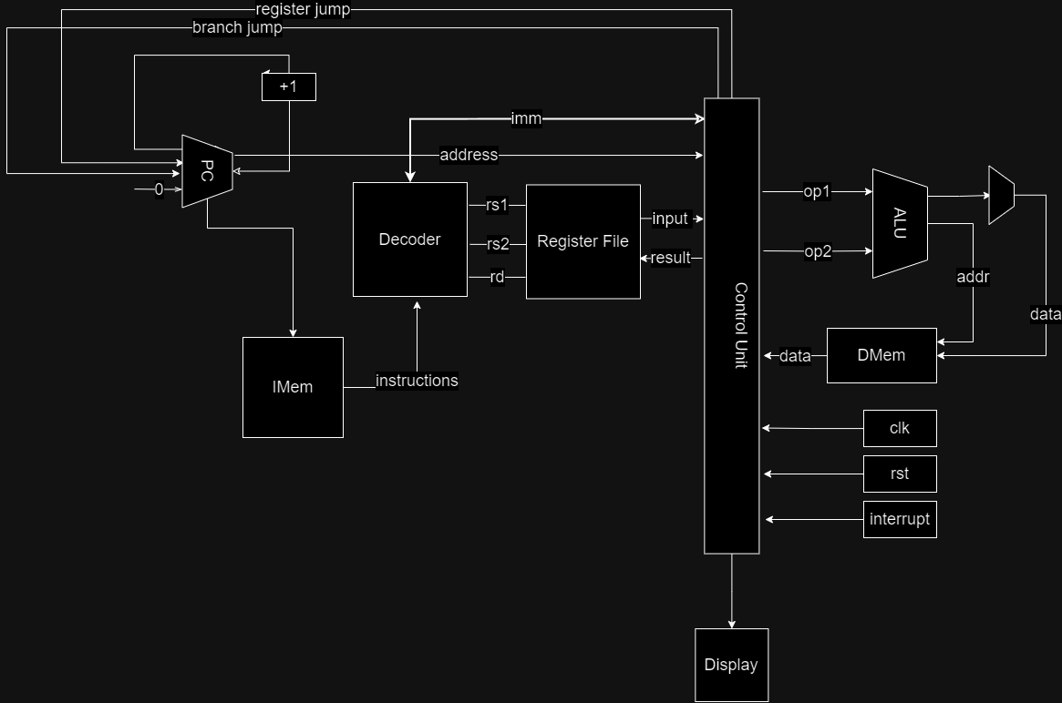
Block diagram of our CPU
Future Task
The job isn’t finished yet as we don’t know whether the whole CPU as a unit performs all of its jobs efficiently and effectively. We plan to use an assembler written in Python (which we already know of) to generate a test code that will test the CPU with all the possibilities instead of hardcoding them into testbench files, this will greatly reduce our efforts and also test our Python skills. With the CPU completely tried and tested we will be integrating the CPU unit into our FPGA through the required software and mark the project as done in our resumes…. Oh wait who’s gonna test if it actually works on FPGA, and what about the OLED display you were talking about… Let’s just focus on the first priority for now.
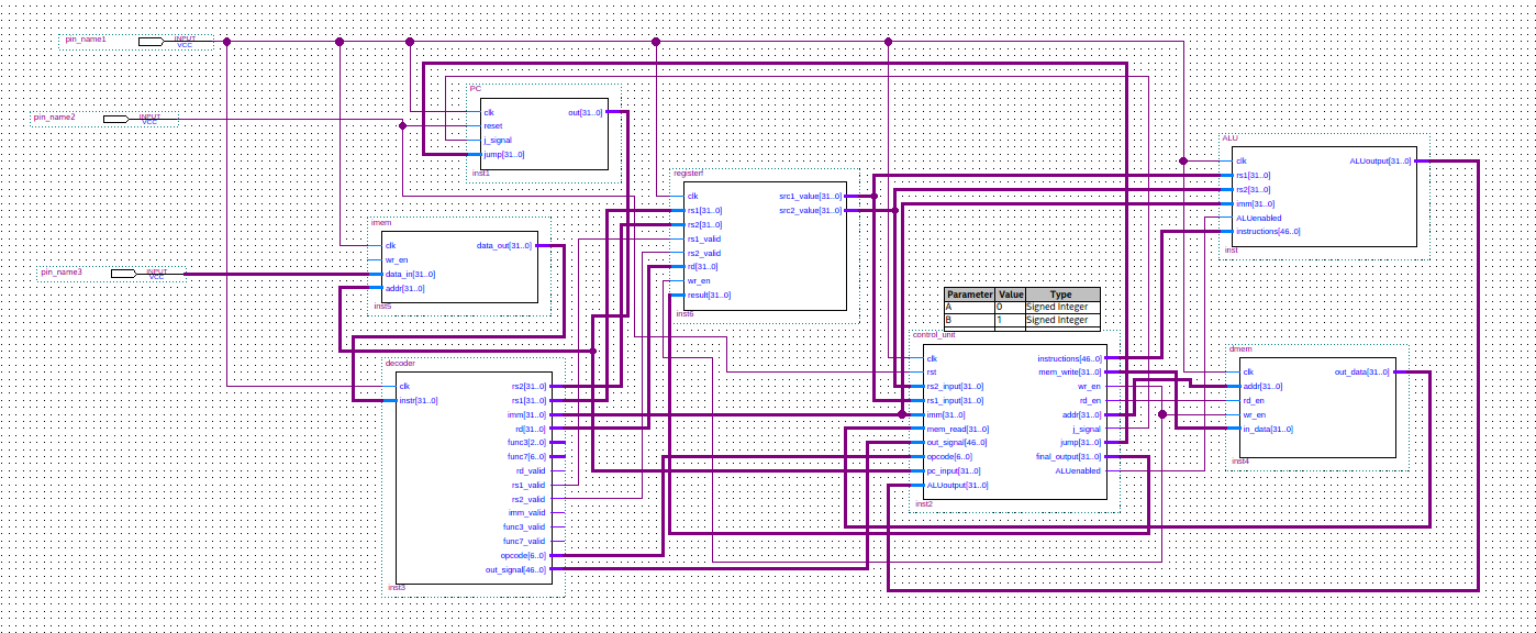
Tentative connections of all Modules of CPU
Problem we Faced:
The first and foremost problem we faced was while testing the written code with their respective testbench as the whole idea of test benches was new to us, generally, we just used the print statements.
The Second problem encountered when we started to suspect if the ALU would be able to perform a complex task like in a mere time of one clock cycle and our suspicions came true for some time when the multiplications for numbers other than two’s powers were incorrect and absolutely misleading, although we later figured out it was just another implementation error and our ALU was doing just fine handling the multiplication task at ease. Once all the basic modules were done we moved to the bigger fish ‘The Control Unit’. The control unit being the center of all the data flow and the key to integrating and binding all the modules together to make a functioning CPU, the module had to be defined perfectly.
This is where we encountered another problem we could not really test the CU module individually, it had to be tested together with all the units combined, which would only make it harder to debug and time-consuming as we later found out it takes almost an hour to synthesize and simulate the whole CPU unit, more over the control unit was a FSM(finite state machine) which would make it even harder to pinpoint the cause of error.
Although thanks to our mentor’s guidance we had a clear idea of how the CU module was going to function we made it do exactly that and we didn’t have to face errors for most of the part. However, there were some times when the thought of punching the laptop crossed our mind as we saw it take a complete hour to compile the code when all we did was add one little line for debugging purposes.
Conclusion:
Facing all the challenges and problems we now have a working CPU(only software synthesized for now), By joining the input-output pins in their correct places and completing the control flow of the CPU we will be moving to our next task and one step closer to having our own working CPU.