 The Society of Robotics and Automation is a society for VJTI students. As the name suggests, we deal with Robotics, Machine Vision and Automation
FPGAs Explained - In 2 Minutes!
What is FPGA?
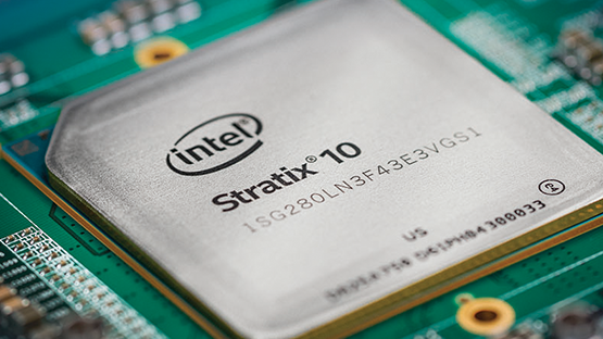
To begin with, FPGA stands for FIELD PROGRAMMABLE GATE ARRAY. it is an Integrated Circuit that can be programmed after manufacture depending upon the application. In a simpler language they are just another semiconductor device that contain programmable logic components(just thousands of logic gates and memory blocks or almost any element) and interconnections . Assume a board contains an FPGA as part of the circuit, it may be programmed during the manufacturing process but can later be re-programmed to reflect any changes depending on the user. Thus it is field programmable, giving rise to its name.
How does FPGA work?
An FPGA by itself does nothing !! Consider it to be a bunch of logic gates and wires, sufficient in amount to make any logic device ranging from a binary adder to a full-fledged CPU Arithmetic Logic Unit. But making a logic device not just requires some IC’s and wires for interconnection. We need to design a logic circuit out of these basic gates to satisfy the needs of our device.
We all know about microcontrollers or microprocessors. Throughout their lifetime, they can perform only a limited number of tasks for which they are designed at the Silicon level. They can only be manipulated at the Software level. For example a microcontroller pin meant for analog input cannot generate a PWM output and vice versa, they are physically restricted within the IC Design.
In contrast to them, FPGA as it’s full form suggests is a reprogrammable device in the sense that the underlying digital design of the device can be reprogrammed as per the user requirements. Yes, you can literally make any I/O pin perform any function, may it be an analog input or a PWM output. You can manipulate an FPGA at the digital hardware level.
The FPGA consists of ‘Configurable Logic Block’ (CLB) i.e. an array of digital designs and are surrounded by programmable ‘Input/ Output Blocks’. There are routing channels that interconnect the different blocks. Additionally, there are multiple Clock signals and Memory blocks within the FPGA.
Good news for the C/C++ haters. FPGAs need a Hardware Description Language (HDL) to code them and believe me people who love digital hardware design will enjoy coding in HDL. No pointers, classes and other complex stuff to deal with. However, it does require great knowledge in digital circuit design and core electronic concepts.
“There ain’t no such thing as a free lunch.”
Hardware Description Languages, as one might assume from the name, are used to describe the layout of a circuit or hardware application. Similar to the relationship of HTML and CSS to web development, Verilog/VHDL have a similar relationship to FPGAs. HDLs can be used to design and describe the layout of digital systems from simple flip-flop memory units to complex communications protocols. The two most popular HDL’s are Verilog and VHDL. We will discuss about them in detail in a separate blog post. Refer to the links provided at the end of this post for a self-start into HDLs.
Why go for FPGAs?
Parallelism : A microcontroller CPU works by dividing it’s computation time between various tasks at hand to make their execution virtually concurrent i.e. parallel execution of various tasks.On the other hand, an FPGA equipped with its hardware layer configurability performs parallel task execution in reality. It is not virtual parallelism, but for real! Scope for making mistakes : When a new IC is designed and fabricated on a Silicon chip there is no room for error by the designers. With an FPGA, the designers can test their designs prior to the fabrication process and optimize the same for better results before actual fabrication starts. This is only due to the hardware reprogrammability of FPGAs. One of the very interesting things about FPGAs is that while you are designing the hardware, you can design the hardware to be a processor that you then can write software for! In fact, companies that design digital circuits, like Intel or nVidia, often use FPGAs to prototype their chips before creating them.
Why not, then?
There are naturally some disadvantages. FPGAs are slower than equivalent ASICs (Application Specific Integrated Circuit) or other equivalent ICs.Also, programming them is not as simple as C programming used in processor based hardware. Additionally they are VERY, VERY EXPENSIVE.
How to design one?
The FPGA design process is started by using a Hardware Description Language (HDL) definition or a schematic design. Common HDLs are VHDL (Very High Speed Integrated Circuit Hardware Description Language) and Verilog. Once this has been completed the next task in the FPGA design process is to produce a netlist for the particular FPGA family being used. The netlist can then be fitted to the actual FPGA architecture using a process called place-and-route. Finally the design is committed to the FPGA and it can be used in the electronic circuit board for which it is intended.
Pretty long post, yeah? It’s actually the result of merging contributions from two authors, that has kept y’all reading for so long.
Yet, there were a lot of assumptions and simplifications made in the explanation to make it lucid enough for beginners. Those who still have the patience to ‘solder’ on, and are interested in diving deep into this topic can surf through the glut of information about FPGAs on Google and the languid ones can just click on the links provided below to get started: (superfluous use of GRE vocab here :p)
To s/w programmers about h/w design
FPGA Architectures: An Overview - Springer